Cart 0
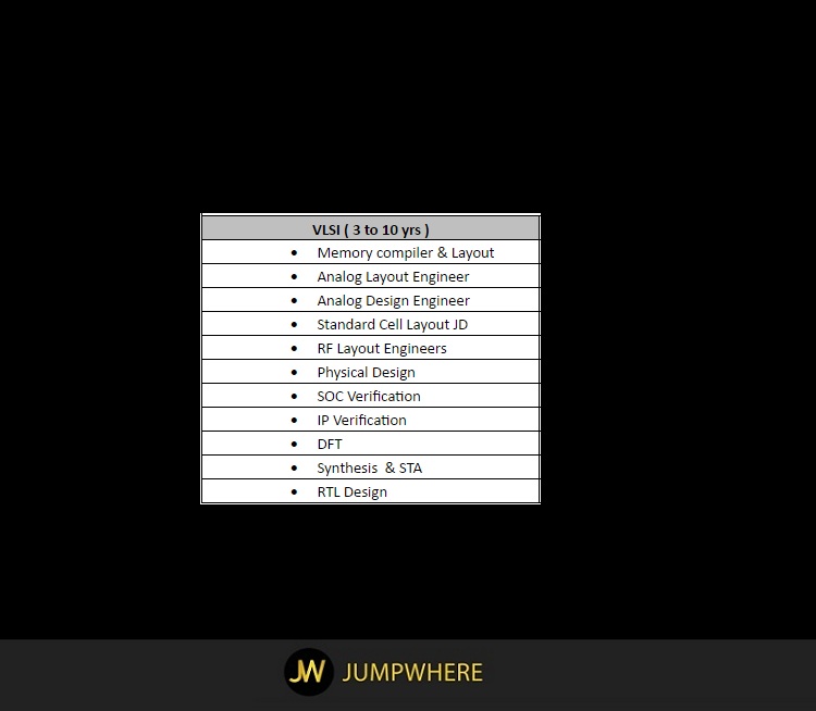
Graphene Semiconductor Services is hiring for multiple positions under VLSI domain. Check below for each of the opening and its job description:
- Minimum experience: 3 years+
- Job location: Bangalore
- Job code: Category Title – Graphene (e.g.: Memory compiler & Layout – Graphene)
- Steps to apply is mentioned at end.
Memory compiler & Layout
Experience: 3-8 years
Bachelor’s Degree Electrical Engineering
Job Description:
- Mask design work on various building blocks of memory or Register file design eg. Drawing mux cells, decoders, memory control, sense amplifiers etc.
• Drawing memory core arrays with proper termination at edges, corners and straps.
• The top level integration of memory instances in memory compiler environment.
• Regression DRC, LVS, density clean-up of memory instances across memory compiler space.
• The IR/EM testing and fixes of memory instances.
Skills required:
- Experience in memory mask design.
- Should have experience working in technologies 45nm and below.
- Should have experience in drawing memory core arrays, write drivers and control circuits.
- Should have sound knowledge of DFM concepts; knowledge of double patterning and coloring concepts are a plus.
- Knowledge of SKILL scripting language is preferred
Analog Layout Engineer
Experience: 4 – 8 yrs
Bachelor’s Degree Electrical Engineering/ Master’s Degree
Job Description:
- 4 years of industry experience in mixed signal CMOS IC layout design at block & chip top level, including chip floor planning and integration
- Must have experience in handling full chip layout and integration using state of the art I.C layout tools
- Experience with Cadence Virtuoso-XL and Mentor Graphics Caliber physical verification tools is a must.
- Experience in DRC, LVS, ERC, Antenna, and post layout extraction.
- Key skills: DRC,LVS,Mixed Signal Layout Design, Analog Layout
Analog Design Engineer
Experience: 2 – 8 yrs
Bachelor’s Degree Electrical Engineering/ Master’s Degree
Job Description:
- You will be a member of the Analog Design team. Your responsibilities will include (but are not limited to):
- Custom circuit design and simulation.
- Custom physical design, extraction, and co-optimization.
- Process, device, template evaluation, and characterization.
- Understand and contribute to methodology development.
- High speed serial/parallel data links (multi Gb/s), PHY circuits, Transceivers, Serializer-Deserializer, PLLs, Clock, and Data Recovery circuits familiarity.
- High speed circuit design in Tx / Rx / Clocking / Reference circuits and low power techniques, silicon reliability, mixed signal design methodology and tools.
- Analog simulators like Cadence, Spice, and System tools like Matlab.
Standard Cell Layout
Experience: 2 – 8 yrs
Bachelor’s Degree Electrical Engineering/ Master’s Degree
Job Description:
- At least 3 years of experience in VLSI layout design or ASIC design automation, CAD tool development and tool integration
- The Candidate will be responsible for Automation of standard cell and custom cell design flow. Automation of standard cell and custom cell library release procedures, customizing tool flows for characterization of standard cells and automation of LPE extraction flow.
- Follow design guidelines set forth by the Engineering and Layout design leads in delivering high quality standard/custom cell layouts in a timely manner.
- In-depth proficiency in sub-micron technologies 28nm, 20soc, 16nm, 14nm, 10nm.
- Good understanding of the standard cell library architecture, ASIC design flow and semi-custom design flows.
- Hands-on layout experience of digital ASICs in leading edge CMOS processes 28nm, 20nm, 16nm, 14nm, 10nm.
- Tools: Cadence (preferably 6.1* Open Access version), Cadence VXL, Mentor Graphics Calibre verification suite, Calibre RVE.
RF Layout Engineers
Experience: 3-6 Years
Bachelor’s Degree Electrical Engineering/ Master’s Degree
Job Description:
- Candidate should work independently on block level and chip level analog layout design, coordinating with the circuit designer & the layout lead .
- Candidate should have 3+ years of hands-on experience in Analog or RF layout.
- Custom layout experience in high frequency circuits such as LNAs, Mixers, VCOs, DAC, ADC, PLL, LDO etc.
- Work closely with the design engineers and layout engineers in designing and successfully delivering analog layouts.
- Full Understanding of IC fabrication and reliability issues.
- Full familiarity with Cadence-Virtuoso, PVS, ASSURA and Calibre tools .
- Knowledge of various analog layout techniques, understanding of various circuit principles as affected by layout such as speed, capacitance, power, noise and area.
- Should have worked on Analog IC Layout, DRC/LVS/Antenna/LPE Checks, CMOS/BiCMOS Device Physics, CMOS/BiCMOS Fabrication Knowledge.
- Outstanding written and verbal communication skills.
Physical Design
Experience : 3 to 12 yrs
Qualification : BE/BTech, ME/MTech ( VLSI Domain )
Location : Bangalore
Role and responsibility:
- Ability to execute block level and SOC level P&R and Timing closure activities.
- Will be responsible for owning up IR/EM/ESD simulations for the various CPU .
- Perform RTL2GDS or Netlist2GDS on blocks and/or fullchip for SoC designs executed by Foundry.
- This design group is designing some of the critical SoCs using Intel foundry design kits.
- The key responsibility is to independently own and converge partitions and sections on 14nm and below processes and execution in converging their blocks for implementation and timing
Job requirements:
- Implementation of multimillion gate SoC designs in cutting edge process technologies (28nm,16nm,14nm & below ).
- Strong Hands-on expertise on any of the aspects of physical design including Synthesis, Floor Planning, Power Plan, Integrated Package and Floorplan design, Place and Route, Clock Planning and Clock Tree Synthesis, complex analog IP integration, Parasitic Extraction, Timing Closure, Power / IR Drop (Static and Dynamic), Signal Integrity Analysis, Physical Verification (DRC, ERC, LVS), DFM and DFY and Tapeout.
- Expertise in analyzing and converging on crosstalk delay, noise glitch, and electrical rules in deep-sub micron processes required. Understanding of process variation effects, and experience in variations analysis/modeling techniques and convergence mechanism would be a plus.
- Expertise in Synopsys IC compiler, Magma or Cadence SOC encounter physical design tools.
- Skill and experience in scripting using Tcl or Perl is highly desirable.
SOC Verification
Experience : 3 to 10 yrs
Qualification : BE/BTech, ME/MTech ( VLSI Domain )
Job Description:
- Development of verification plans
- Verification environments
- Test cases and ensuring coverage and performance goals are achieved for IP and SOC level.
- Working Knowledge of ARM processors.
- HVLs/Tools: SV, UVM, C
- Domain: Networking, DDR2/3/4, Ethernet PCIe
IP Verification
Experience: 3 to 10 yrs
Qualification : BE/BTech, ME/MTech ( VLSI Domain )
Job Description:
- 4 – 10 years experience in Design Verification
- Strong System Verilog or Specman expertise OVM/UVM/eRM expertise highly desired
- Good knowledge of protocols
- Ability and desire to learn new methodologies, languages, protocols etc
DFT
Experience : 3 to 10 yrs
Qualification : BE/BTech, ME/MTech ( VLSI Domain )
Job Description:
- Strong knowledge and experience in Scan Insertion, TestKompression, ATPG, Memory BIST and JTAG at IC –level for mixed signal designs.
- Experience in using Mentor DfT tools, Cadence RC and simulator tools
- Define DfT Strategy and Requirement Specification for the design
- DfT verification for gate-level and timing simulations
- Work cross sites with design team to define and implement DfT.
- Hands on experience in solving DfT problems, simulation failures, ATPG coverage and DRC improvements.
- Work with STA engineer to define timing constraints for DfT modes
- Support Test engineer in silicon debug and pattern delivery for ATE
- Experience in RTL coding, shell scripting
- Experienced in handling analog DfT simulations
- Be fluent with all common concepts of DfT and DfT tools
Synthesis/STA
Experience: 3 to 10 yrs
Qualification: BE/BTech, ME/MTech ( VLSI Domain )
Job Description:
- Expertise in Synthesis using Synopsys DC/ Cadence RTL Compiler based tool set
- Expertise in Synthesis for High Performance , Low Power, Low Area based Flows
- Expertise in SDC Constraints Creation and constraints cleanup based on the timing issues
- Expertise in Formal & Low Power Verification using Synopsys/Cadence based tools
- Expertise in Running PTSI/ETS tools for Timing Sign-off and generating timing ECO based on the timing issues
- Expertise in Multi-mode multi-corner STA analysis on SoC
- Skill and experience in scripting using Tcl or Perl is highly desirable.
RTL Design
Experience : 3 to 10 yrs
Qualification : BE/BTech, ME/MTech ( VLSI Domain )
Job Description:
- Good understanding of Multi-processor and cache designs Hands on coding experience in Verilog/VHDL
- Familiarity with various ARM AMBA protocols (e.g AXI, AHB etc) as well as cache coherency protocols
- Has good knowledge on various tools viz Spyglass, 0-in, DC-Compiler, Prime time, PTPX, Power-Artist,LEC etc
- Working knowledge of timing closure is a plus Expertise in Perl, TCL language is a plus.
How to apply for this Job Opening?
For more information upload your resume here with proper job code, subject and details.Other openings can be checked in Job Vacancies
Note: Only shortlisted candidates will get a call for interview.